


About QUICK

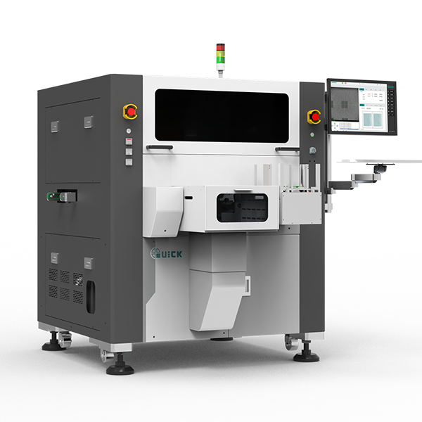
Thermo-Compression Bonder
AI
High performance computing
High Speed Die Bonder
Discrete device
Integrated circuit
MEMS, Transducer
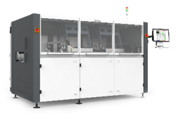
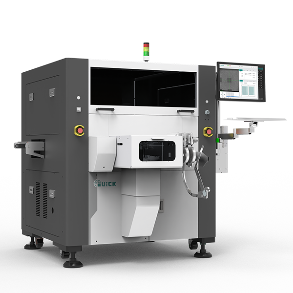
Thermo-compression Die Bonder
Power semiconductor
New energy vehicle
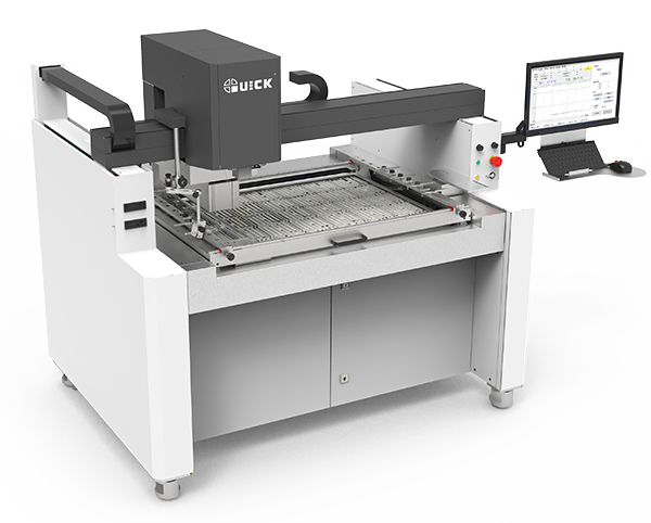
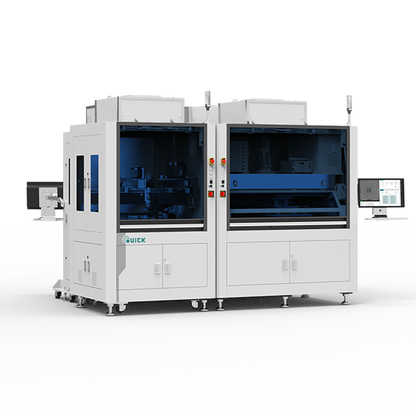
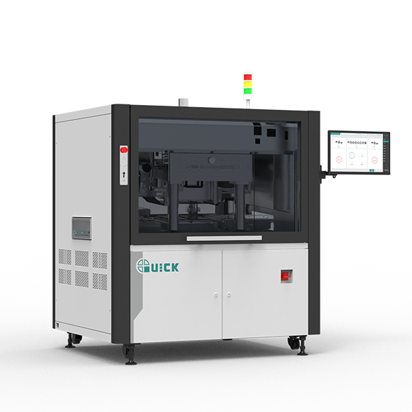
Multifunctional Die Bonder
Power semiconductor
New energy vehicle
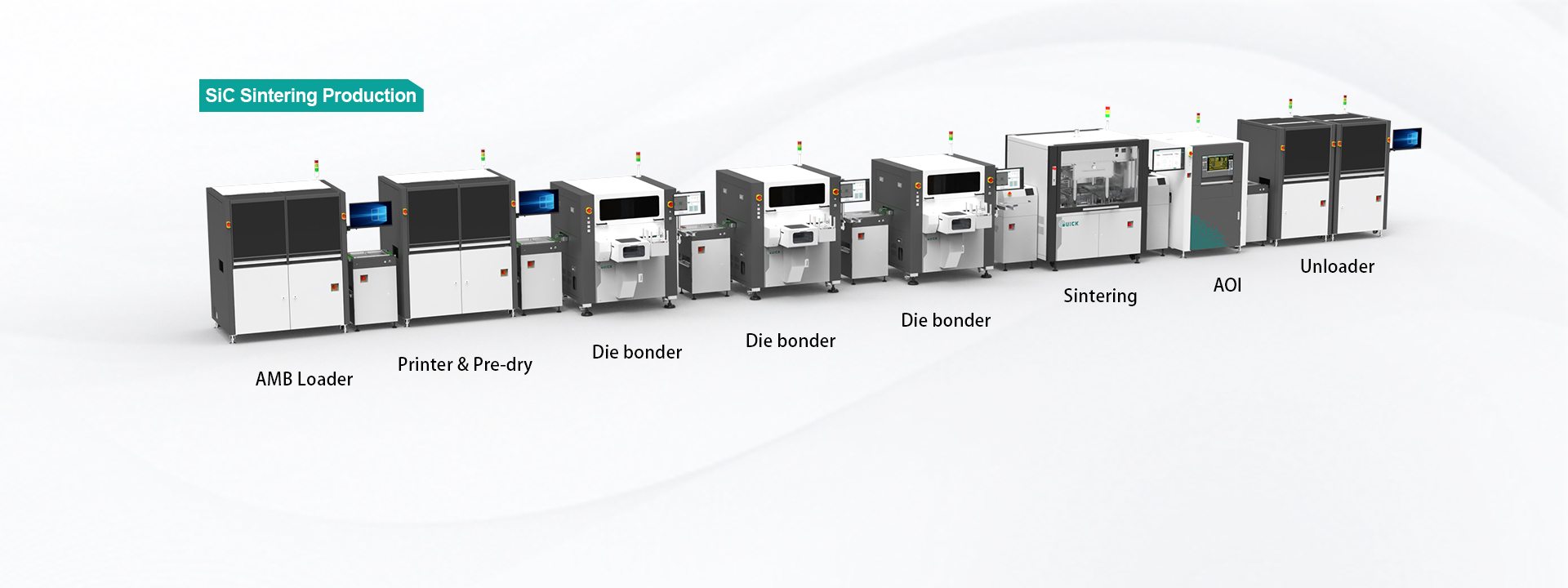
Silver Sintering
Power semiconductor
New energy vehicle
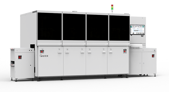
Vacuum Oven
Power semiconductor
Automotive
Aerospace
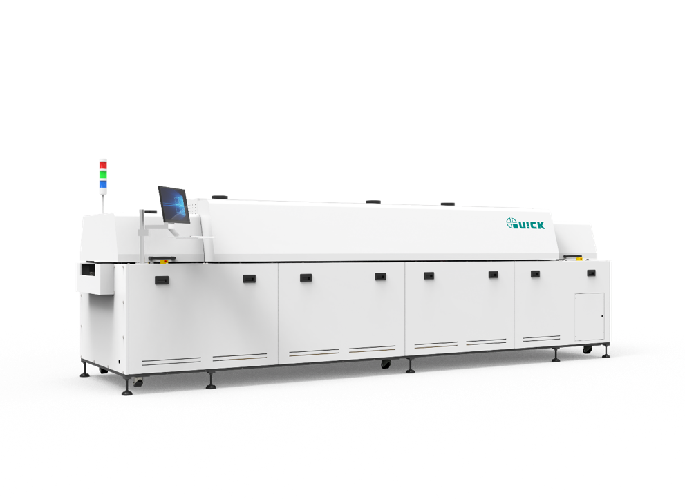
Formic Acid Oven
Power Semiconductor
Automotive
Industrial
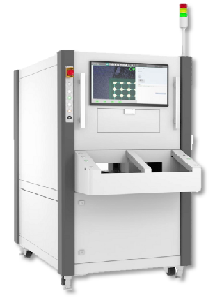
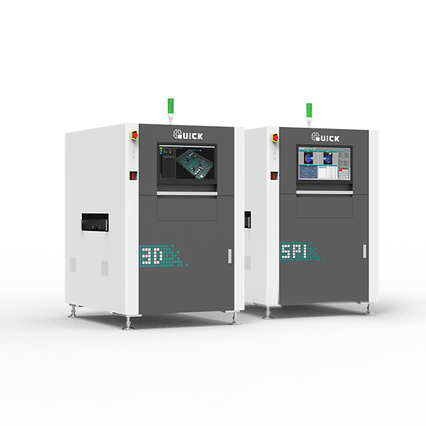
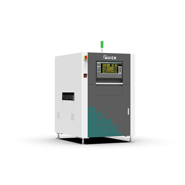
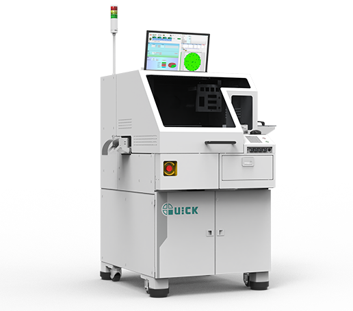
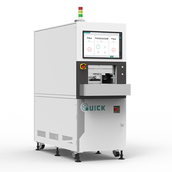
Die Packaging AOI
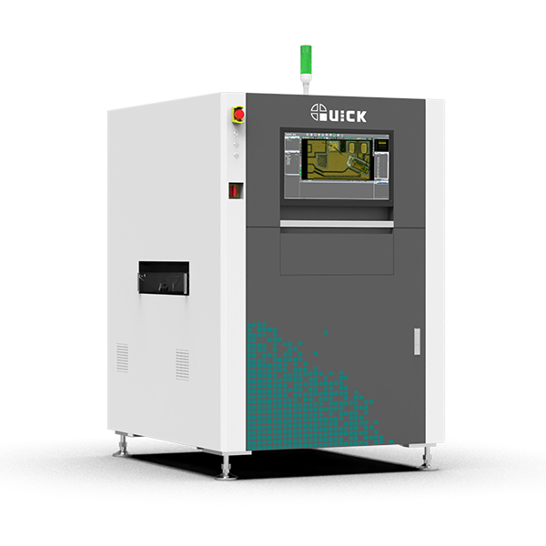
Photoelectric Component
Power Module
T/R Module
Die Packaging

PAY ATTENTION TO US
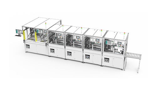
Soldering assembly/visual process
Intelligent terminal and Intelligent wear
New energy
Semiconductor
Electro-optic display
About QUICK


